
Some time ago I Emailed a columnist at ” Monitoring Times” and said that I did not think a schematic printed in the column that month for an inverter would work. The inverter schematic looks like one that was printed in a 1960 “Motorola Power Transistor Handbook” first edition page 115 and 125. I think it only fair if I say some ones circuit will not work I should come up with one that does.
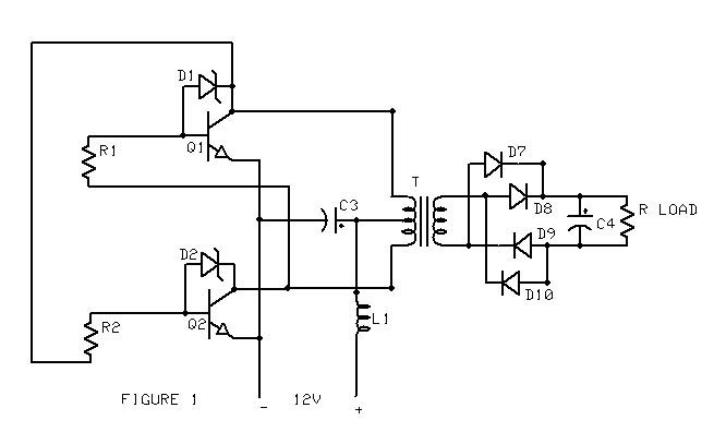
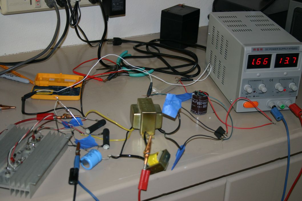
The schematic in the column showed two transformers with the secondary’s in series which would not provide any base drive to the transistors. The Motorola schematic used a single transformer with a center tapped primary, this will provide base drive. The Motorola article specified the use of 2N176 transistors which were a 1956 germanium design and to the best of my knowledge are no longer made. I don’t know of any source for germanium power transistors. I had two 30 year old silicon power transistors mounted on a heat sink so I started with these. They were 2N3055s. 2N3055s would have been my first choice for this inverter even if I had not had two already mounted on a heat sink, 2N3055s are cheap, rugged, and have a 15 amp rating. FIGURE 1 shows the first test of this inverter circuit. The only change from the Motorola circuit is the addition of Zener diodes from the base to the collector of the transistors. These diodes will catch any high voltage spikes that may appear at the transistor collectors due to inductive kick at turn off time. The diode selected is a 51 volt unit which conducts below the voltage rating of the transistor. At around 51 volts the transistor will turn on clamping the spike and dissipating the energy in it. This will prevent the high voltage spike from breaking down the transistor junctions which will eventually destroy the transistors. Also a bypass capacitor and filter choke were added at the power input point. The capacitor provides an
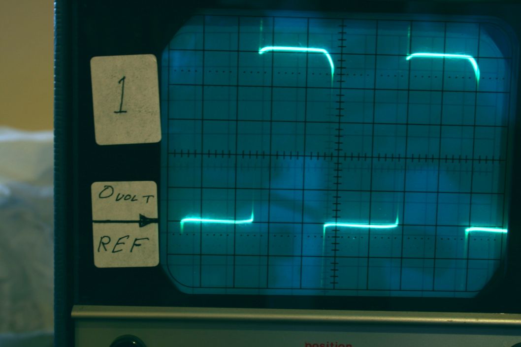
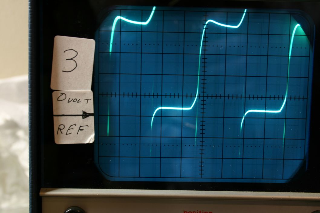
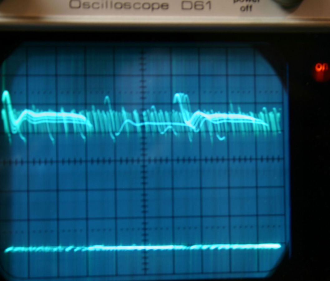
AC return at the inverter circuit rather than at the power supply which may be several feet from the inverter. The choke isolates the inverter from the power supply. This keeps inverter noise out of the power supply and protects the inverter transistors from large transient voltages that may appear on the power supply such as found in automotive applications. Oscilloscope pictures 1 through 5 were shot with 13.8 volts in and a 4K load. Scope picture #1 shows the collector to emitter wave form in FIGURE 1. Scale is 5Volts/ div. This picture shows the large positive voltage spike which goes off screen but is being clamped at 50 volts by the Zener and transistor. There is also a negative spike on turn on. This negative spike probably is causing the base emitter junction to break down like a Zener. I have been told this is not good for a transistor although I have not seen a good explanation of why. I have seen a transistor used as a Zener in a TV voltage regulator. Scope picture #2 shows
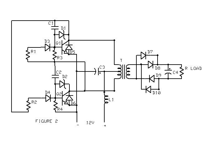
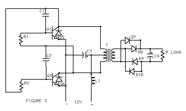
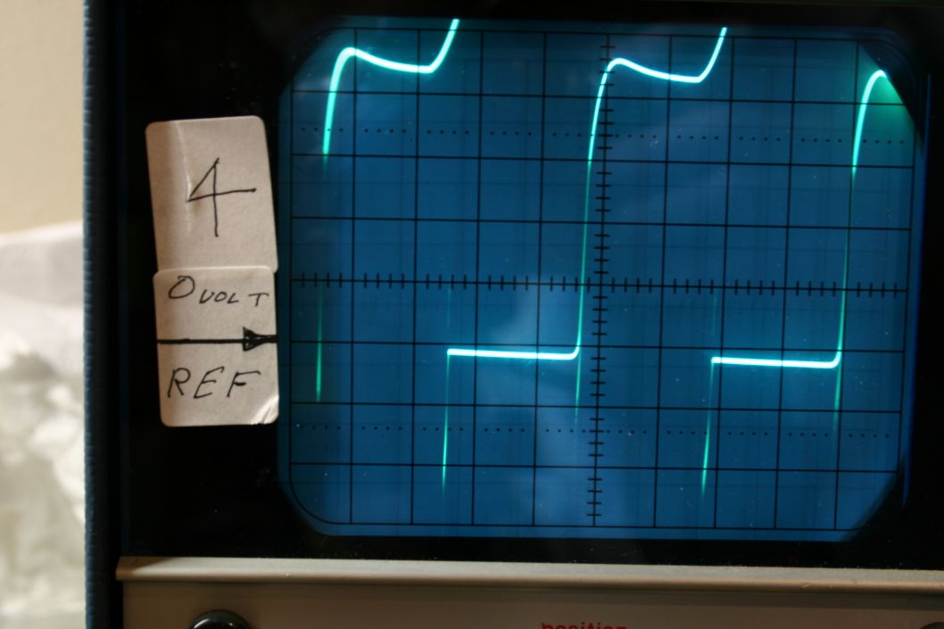
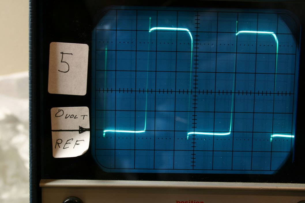
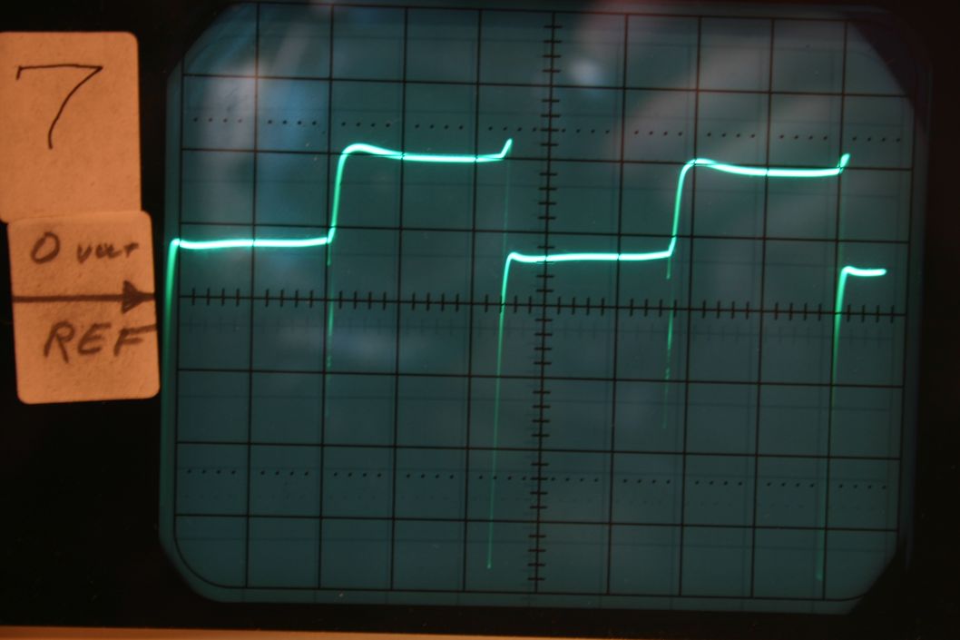
The addition of diodes D5 and D6 to clamp the negative spike. Ref. FIGURE 2. Scale is 5Volts/div. Scope picture #3 shows the wave form from base to emitter. Scale .2Volts/div. The “off” transistor depends on the “on” transistor to have a saturation voltage lower than the turn on voltage of the “off” transistor. For a silicon transistor the turn on voltage is usually around .6 volts. The voltage at the base of the “off “transistor as shown in scope picture #3 shows the base voltage to be .08 volts when the transistor is off. The saturation voltage of the “on” transistor is proportional to the current flowing through the transistor so if the load on the inverter is increased the saturation voltage will increase. The saturation voltage(resistance) is different with each type of transistor. Higher voltage types usually have a higher saturation resistance. An experiment was tried to increase the safety margin and assure the “off” transistor was indeed off. Diodes D3 and D4 were added in series with the base of the transistors, this added another .6 volt drop to the saturation voltage of the “on” transistor. Because the base of the “off” transistor would be left floating resistors R3 and R4 were added to pull the base to 0volts. Scope picture #4 shows the base emitter wave form with D3,D4,R3, and R4 added. Scale .2Volts/div. With the transistors I used these parts are not necessary with an input current below 5 amps. If the transistors used do not saturate below .6 volts the “off” transistor will turn on and dissipate a large amount of power. The “off” transistor will have twice the supply voltage on the collector so any current flow will cause a large amount of dissipation . One unlabeled scope picture shows a high frequency oscillation when the inverter was heavily loaded at turn on. This picture shows the waveform from collector to emitter scaled at 5Volts/div. This high frequency oscillation always occurred at turn on when C4 was discharged and then go away and settle into a low frequency flux controlled mode as it charged if Rload was 4K or greater. With a 2K or 1.33K load the high frequency oscillation would continue with the inverter putting out very low power and heating the transistors. A nearby scanner picked up harmonics as high as 40 Mhz. The frequency of oscillation must be in a region where the coupling between the primary and secondary of the transformer is rather loose. (My guess). This problem probably never occurred with the original Motorola circuit with the 2N176 transistors. The 2N176 transistor has a fae of 7Khz where the 2N3055 has a fae of 800Khz. The 2N3055 takes of in this high frequency mode because it can. Slowing down the 2N 3055s fixed this problem. .047uf capacitors were connected from Base to collectors of the transistors.(C1 and C2). With different loads, transformers, or transistor types larger capacitors may be required to halt the high frequency oscillation. When powering tube circuits there should be no problem as the inverter should calm down into a flux oscillation mode before the tubes light up and start drawing current. When the capacitors C1 and C2 were added they caused the transistors to clamp the high voltage spike at turn off so with the capacitors added Zener diodes D1 and D2 are no longer required. Scope picture # 5 shows the collector to emitter waveform with C1 and C2 added. Note the high voltage positive spike is clamped. Scale is 5Volts/div. FIGURE 3 shows the final schematic of what I consider a practical inverter using the basic circuit printed in “Monitoring Times”. Scope pictures #6 and #7 show waveforms with the circuit configured as per FIGURE 3 with 13.8volts in at 4.2 amps and 205 volts out at 153ma into 1.333K. Scope picture #6 shows the collector to emitter wave form. Scale 5Volts/div. Scope picture #7 shows the base to emitter wave form. Scale .5Volts/div. Note the base emitter voltage when “off” has risen to .35 volts due to the greater transistor current than was flowing in scope picture # 3.


PARTS LIST
Q1,Q2 2N3055
R1,R2 100 ohms 10 watt
R3,R4 100 ohms 1/4 watt
D1,D2 51 volt 1 watt zener diode 1N4757
D3,D4,D5,D6 1N4007, HEP170, Radio Shack 276-1114
D7,D8,D9,D10 4 amp 600 volt bridge or 1N4007, HEP170, Radio Shack 276-1114
C1,C2 .047uf 250 volt
C3 1000uf 40 volt
C4 330uf 400volt
L1 Radio Shack filter choke 270-030
T Archer 273-1511 120v to 12.6v at 3 amps
